MIT.nano
October 13, 2022
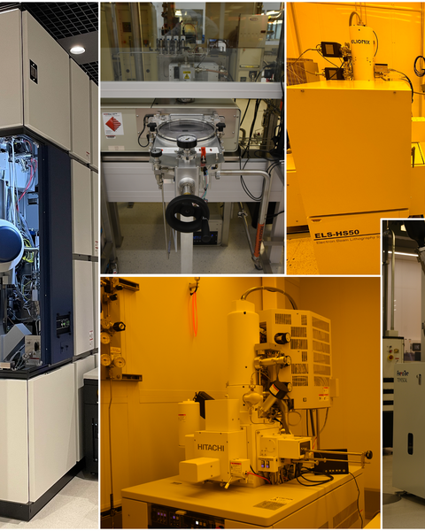
MIT.nano has added several instruments to its tool set, expanding the facilities’ capabilities at the nanoscale. The tools, located in MIT.nano’s cleanroom and characterization spaces, can be used individually, or they might all be utilized during different stages of one complete project.
“Overall, these tools are important additions to MIT.nano that will help researchers create and analyze at the nanoscale,” says Jorg Scholvin, assistant director for Fab.nano. “Each fills a critical gap in our existing set of capabilities. What’s really exciting is the range — they can all handle the smallest pieces up to 200-millimeter wafers.”
New tools installed at MIT.nano include the Hitachi HF5000 environmental transmission electron microscope, the Arradiance GEMStar ALD system, the Elionix HS50, the Temescal FC-2800 e-beam evaporator, and the Hitachi Regulus 8100 scanning-electron microscope.
Complete article from MIT News.
Explore
MIT Researchers use AI to Uncover Atomic Defects in Materials
Zach Winn | MIT News
A new model measures defects that can be leveraged to improve materials’ mechanical strength, heat transfer, and energy-conversion efficiency.
“Near-misses” in Particle Accelerators can Illuminate New Physics, Study finds
Jennifer Chu | MIT News
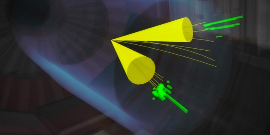
Physicists discovered new properties of the strong force by analyzing what happens when light-speed particles skim by each other.
Why Solid-state Batteries Keep Short-circuiting
Zach Winn | MIT News
New insights into metallic cracks that harm battery performance could advance the longstanding quest to develop energy-dense solid-state batteries.


