
Despite the much debated end of Moore’s Law, CMOS scaling still maintains economic relevance with 3nm finFET SoCs already in the marketplace for over a year and 2nm gate-all around SoCs well into risk production. Modest feature size reduction and design/technology innovations co-optimized for primarily logic scaling continue to offer compelling node-to-node power, performance, area, and cost benefits. In this tutorial, we will start with a walk through memory lane, recounting a brief history of transistor evolution to motivate the migration from the planar MOSFET to the fully depleted FinFET. We will summarize the key process technology elements that have enabled the finFET CMOS nodes, highlighting the resulting device technology characteristics and challenges. This will set the context for motivating the introduction of the gate-all-around device architecture, namely nanoribbons or nanosheets, and unveiling the magic of how these devices are fabricated.
This webinar is part of the MIT Circuits and Systems Seminar Series.

Speaker
Alvin Loke
Alvin Loke is a Senior Principal Engineer at Intel working on analog design/technology co optimization of Intel’s Angstrom-era nodes. He received his PhDEE from Stanford and has worked on CMOS nodes from 250nm to 1nm. His experience covers CMOS process integration to analog/mixed-signal and wireline design as well as design/model/technology interfacing. He has previously worked at Agilent Technologies, AMD, Qualcomm, TSMC and NXP Semiconductors. Since 2003, Alvin has served multiple roles in the IEEE Solid-State Circuits Society including Distinguished Lecturer, AdCom Member, Guest Editor, and currently Global Chapters Chair.
Explore
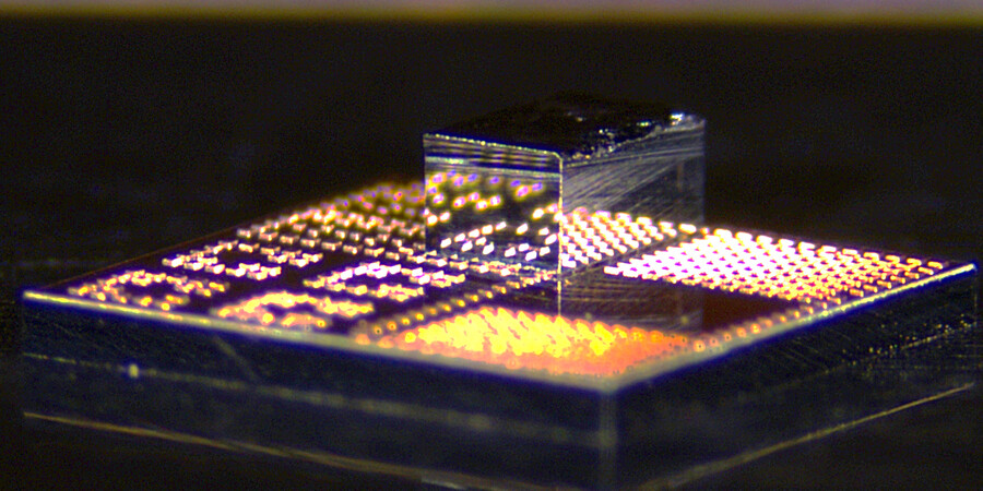
New 3D Chips could Make Electronics Faster and more Energy-Efficient
Adam Zewe | MIT News
The low-cost, scalable technology can seamlessly integrate high-speed gallium nitride transistors onto a standard silicon chip.

Anantha Chandrakasan Named MIT Provost
Kathy Wren | MIT News
A faculty member since 1994, Chandrakasan has also served as dean of engineering and MIT’s inaugural chief innovation and strategy officer, among other roles.

Photonic Processor could Streamline 6G Wireless Signal Processing
Adam Zewe | MIT News
By performing deep learning at the speed of light, this chip could give edge devices new capabilities for real-time data analysis.