
Explore
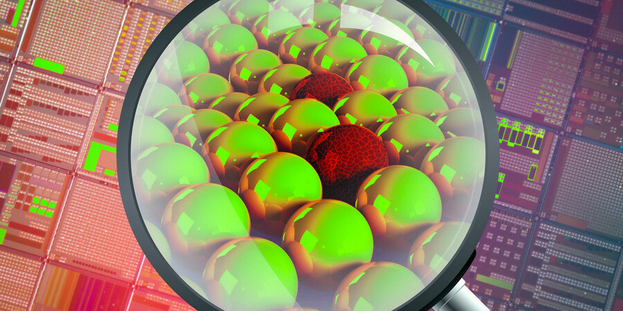
MIT Researchers use AI to Uncover Atomic Defects in Materials
Zach Winn | MIT News
A new model measures defects that can be leveraged to improve materials’ mechanical strength, heat transfer, and energy-conversion efficiency.
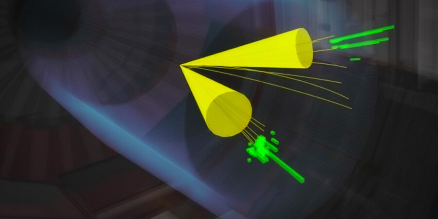
“Near-misses” in Particle Accelerators can Illuminate New Physics, Study finds
Jennifer Chu | MIT News
Physicists discovered new properties of the strong force by analyzing what happens when light-speed particles skim by each other.
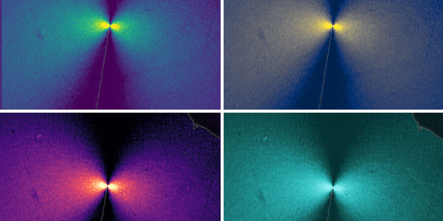
Why Solid-state Batteries Keep Short-circuiting
Zach Winn | MIT News
New insights into metallic cracks that harm battery performance could advance the longstanding quest to develop energy-dense solid-state batteries.