April 27, 2023
Emerging AI applications, like chatbots that generate natural human language, demand denser, more powerful computer chips. But semiconductor chips are traditionally made with bulk materials, which are boxy 3D structures, so stacking multiple layers of transistors to create denser integrations is very difficult.
However, semiconductor transistors made from ultrathin 2D materials, each only about three atoms in thickness, could be stacked up to create more powerful chips. To this end, MIT researchers have now demonstrated a novel technology that can effectively and efficiently “grow” layers of 2D transition metal dichalcogenide (TMD) materials directly on top of a fully fabricated silicon chip to enable denser integrations.
Growing 2D materials directly onto a silicon CMOS wafer has posed a major challenge because the process usually requires temperatures of about 600 degrees Celsius, while silicon transistors and circuits could break down when heated above 400 degrees. Now, the interdisciplinary team of MIT researchers has developed a low-temperature growth process that does not damage the chip. The technology allows 2D semiconductor transistors to be directly integrated on top of standard silicon circuits.
Complete article from MIT News.
Explore
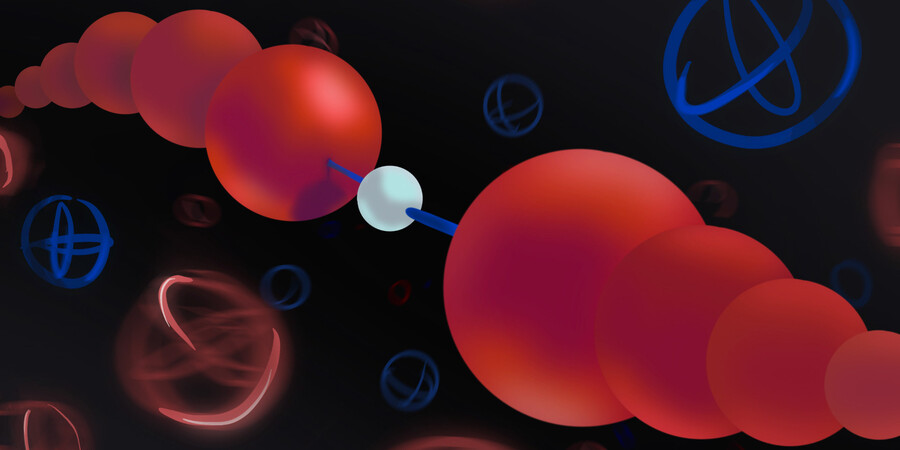
What Makes a Good Proton Conductor?
Zach Winn | MIT News
MIT researchers found a way to predict how efficiently materials can transport protons in clean energy devices and other advanced technologies.
Lisa Su ’90, SM ’91, PhD ’94 to deliver MIT’s 2026 Commencement address
Kathy Wren | MIT News
An electrical engineer by training, Su is the chair and CEO of the semiconductor company AMD.
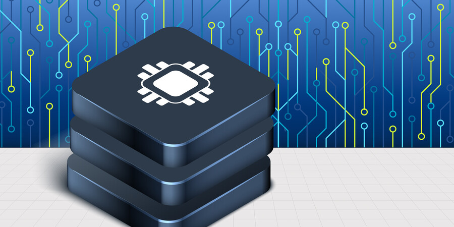
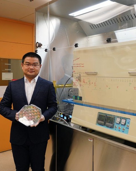
New Materials Could Boost the Energy Efficiency of Microelectronics
Adam Zewe | MIT News
By stacking multiple active components based on new materials on the back end of a computer chip, this new approach reduces the amount of energy wasted during computation.


