January 30, 2024
A new set of advanced nanofabrication equipment will make MIT.nano one of the world’s most advanced research facilities in microelectronics and related technologies, unlocking new opportunities for experimentation and widening the path for promising inventions to become impactful new products.
The equipment, provided by Applied Materials, will significantly expand MIT.nano’s nanofabrication capabilities, making them compatible with wafers — thin, round slices of semiconductor material — up to 200 millimeters, or 8 inches, in diameter, a size widely used in industry. The new tools will allow researchers to prototype a vast array of new microelectronic devices using state-of-the-art materials and fabrication processes. At the same time, the 200-millimeter compatibility will support close collaboration with industry and enable innovations to be rapidly adopted by companies and mass produced.
MIT.nano’s leaders say the equipment, which will also be available to scientists outside of MIT, will dramatically enhance their facility’s capabilities, allowing experts in the region to more efficiently explore new approaches in “tough tech” sectors, including advanced electronics, next-generation batteries, renewable energies, optical computing, biological sensing, and a host of other areas — many likely yet to be imagined.
Complete article from MIT News.
Explore
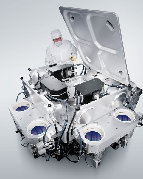
Tomás Palacios appointed Director of ISN
Office of the Vice President for Research
As director, Tomás will lead ISN’s research mission and build communities within MIT and with external partners.
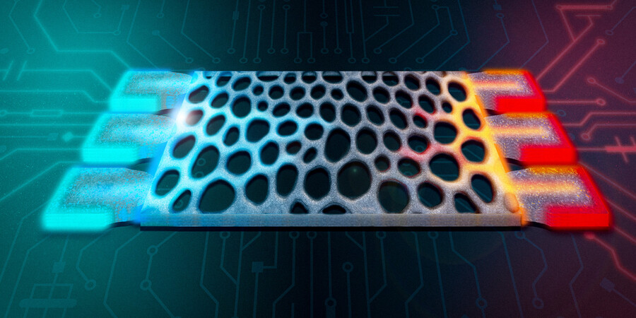
MIT Engineers Design Structures that Compute with Heat
Adam Zewe | MIT News
By leveraging excess heat instead of electricity, microscopic silicon structures could enable more energy-efficient thermal sensing and signal processing.
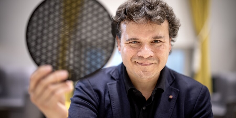
Pablo Jarillo-Herrero wins BBVA Foundation Frontiers of Knowledge Award
MIT physicist shares award for influential work on “magic-angle” graphene.
Materials Research Laboratory


