Friday, November 5, 2021 | 11:00am-12:00pm ET
Speaker: Dr. Jeffrey L. Burns, IBM Research
Please use this link to view a recording of the MIT AI Hardware Program seminar
Please use this link to view event slides
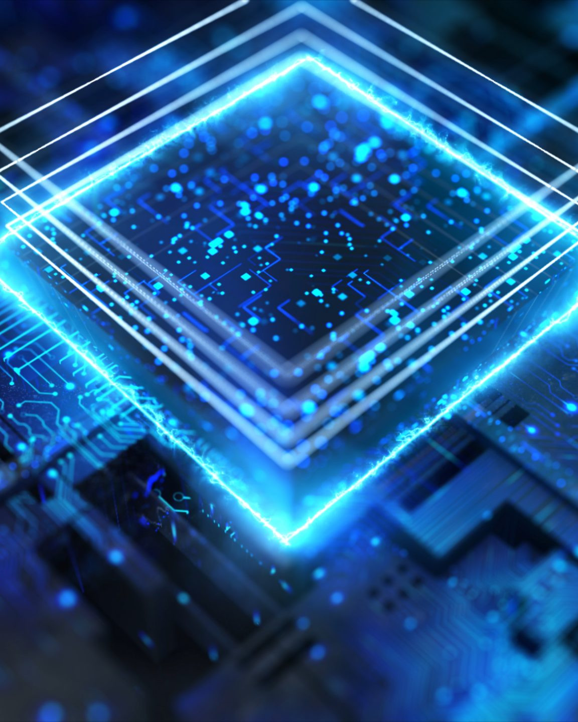
Abstract: The need for consuming/processing different kinds of unstructured data such as natural language data and image data has gone up exponentially, with deep learning (DL) based AI algorithms being deployed for this purpose. Since DL algorithms are noise resilient and use mathematical operations (such as matrix-matrix multiplications) that are repeated, they benefit from a high degree of parallel processing. This has led to explosive growth in the use of GPUs and ASICs for DL, though at the expense of significant burdens in energy consumption and computation time. To address the challenges and opportunities of AI computing, the IBM Research AI Hardware Center has developed an end to end compute paradigm to enhance compute efficiency and improve throughput performance. This includes leveraging novel algorithmic ideas such as arithmetic precision scaling and concomitant chip architectures while maintaining iso-accuracy; novel Analog In-Memory Compute architectures with artificial neural networks mapped on to arrays of non-volatile memory (NVM) elements; and Heterogeneous Integration (HI) and advanced packaging technologies that leverage these compute paradigms to realize balanced system level performance. In addition, we provide an integrated AI-software stack and infrastructure that enables libraries, simulation, and emulation software to size the hardware benefits and to develop use cases. This presentation will cover these research initiatives we are pursuing in the Center.
 Speaker Bio: Jeffrey Burns is the Director of the IBM Research AI Hardware Center. He manages the Center’s activities across materials, advanced packaging, accelerator design, software, and applications. Upon joining IBM Research at the T.J. Watson Research Center he initially worked in layout automation and processor design. Subsequently he has managed teams and projects in VLSI design, design automation, microprocessors, systems architecture, and AI. He received his B.S. in Engineering from UCLA, and his M.S. and Ph.D. in Electrical Engineering from U.C. Berkeley.
Explore

Tomás Palacios appointed Director of ISN
Office of the Vice President for Research
As director, Tomás will lead ISN’s research mission and build communities within MIT and with external partners.

Lisa Su ’90, SM ’91, PhD ’94 to deliver MIT’s 2026 Commencement address
Kathy Wren | MIT News
An electrical engineer by training, Su is the chair and CEO of the semiconductor company AMD.
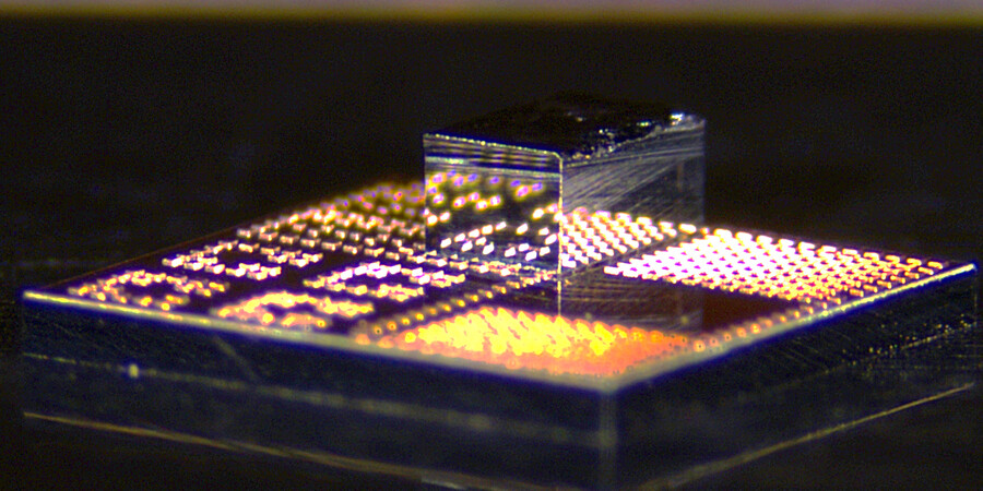
New 3D Chips could Make Electronics Faster and more Energy-Efficient
Adam Zewe | MIT News
The low-cost, scalable technology can seamlessly integrate high-speed gallium nitride transistors onto a standard silicon chip.