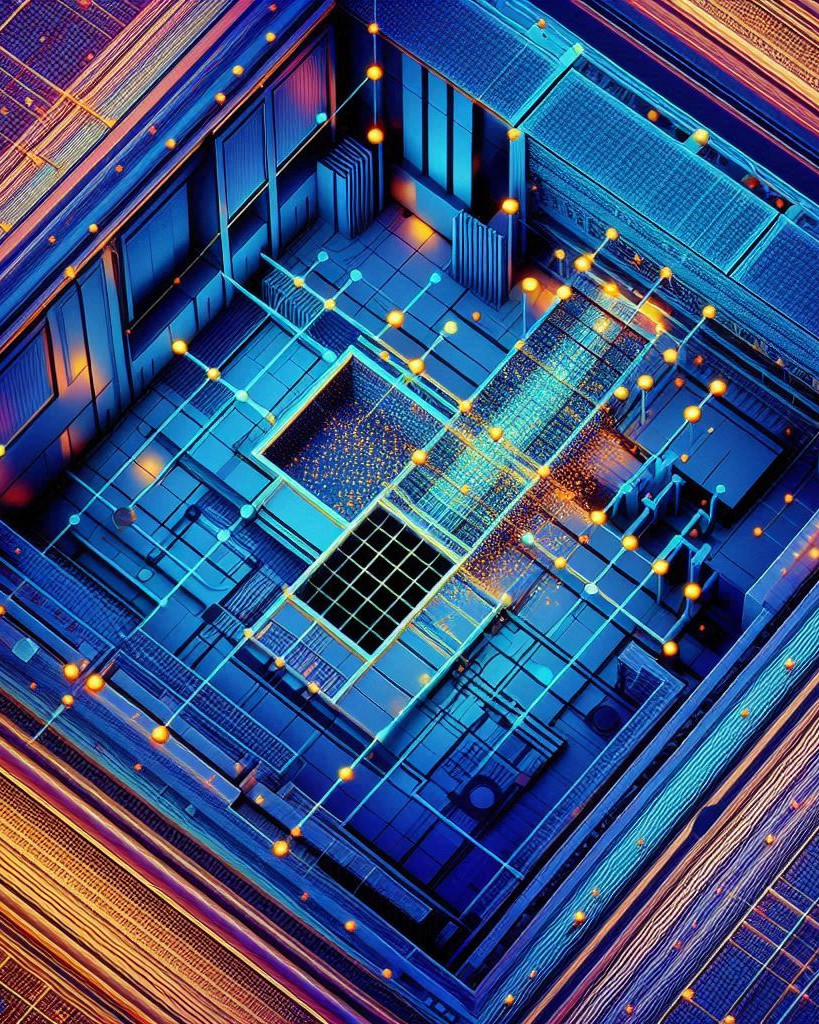
EUV lithography is now used to manufacture the most advanced integrated circuits, including memory, logic and AI chips, but Moore’s Law demands constant improvements. The NXE system is our 0.33NA platform which continues to evolve with better throughput via greater EUV source power, smaller Edge Placement Errors (EPE) and higher uptime. One possibility for further EPE reduction is to increase image contrast through the use of advanced exposure methods such as Dual Monopole.

Speaker
Tim Brunner
Tim Brunner holds a B.A. from Carleton College and a Ph.D from MIT, all in physics. He has worked in the area of lithography for chip production since 1981. After many years at IBM, he joined ASML in 2019, working in the Technology Development Center.
Explore
What Makes a Good Proton Conductor?
Zach Winn | MIT News
MIT researchers found a way to predict how efficiently materials can transport protons in clean energy devices and other advanced technologies.

Lisa Su ’90, SM ’91, PhD ’94 to deliver MIT’s 2026 Commencement address
Kathy Wren | MIT News
An electrical engineer by training, Su is the chair and CEO of the semiconductor company AMD.
New Materials Could Boost the Energy Efficiency of Microelectronics
Adam Zewe | MIT News
By stacking multiple active components based on new materials on the back end of a computer chip, this new approach reduces the amount of energy wasted during computation.