
April 27, 2023
Emerging AI applications, like chatbots that generate natural human language, demand denser, more powerful computer chips. But semiconductor chips are traditionally made with bulk materials, which are boxy 3D structures, so stacking multiple layers of transistors to create denser integrations is very difficult.
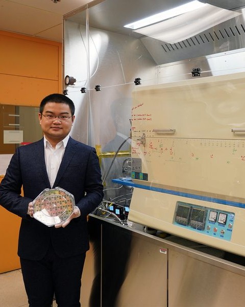
However, semiconductor transistors made from ultrathin 2D materials, each only about three atoms in thickness, could be stacked up to create more powerful chips. To this end, MIT researchers have now demonstrated a novel technology that can effectively and efficiently “grow” layers of 2D transition metal dichalcogenide (TMD) materials directly on top of a fully fabricated silicon chip to enable denser integrations.
Growing 2D materials directly onto a silicon CMOS wafer has posed a major challenge because the process usually requires temperatures of about 600 degrees Celsius, while silicon transistors and circuits could break down when heated above 400 degrees. Now, the interdisciplinary team of MIT researchers has developed a low-temperature growth process that does not damage the chip. The technology allows 2D semiconductor transistors to be directly integrated on top of standard silicon circuits.
Complete article from MIT News.
Explore
Discovery helps explain why solid-state batteries often fail
Zach Winn | MIT News
New research could help prevent the formation of tiny seeds of lithium metal within the electrolyte, enabling batteries that charge faster and last longer.

MIT researchers advance toward greater bandwidth, more energy-efficient communications
Elizabeth A. Thomson | Materials Research Laboratory
The FUTUR-IC research program integrates electronics and photonics in microchip systems.

Graphene can hold multiple states of superconductivity, a new study finds
Jennifer Chu | MIT News
What’s more, the superconducting states get stronger under conditions expected to kill them.


