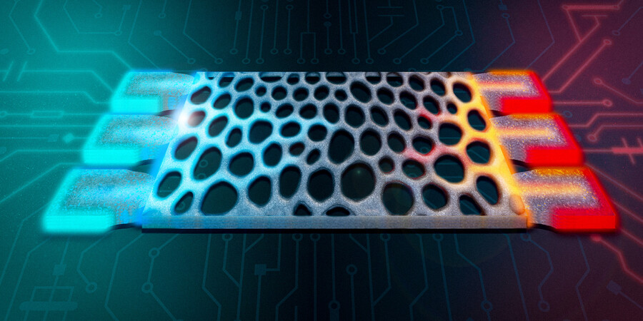
December 11, 2025
MIT researchers have developed a new fabrication method that could enable the production of more energy efficient electronics by stacking multiple functional components on top of one existing circuit.
In traditional circuits, logic devices that perform computation, like transistors, and memory devices that store data are built as separate components, forcing data to travel back and forth between them, which wastes energy.
This new electronics integration platform allows scientists to fabricate transistors and memory devices in one compact stack on a semiconductor chip. This eliminates much of that wasted energy while boosting the speed of computation.
Complete article from MIT News.
Explore
MIT Physicists Observe Key Evidence of Unconventional Superconductivity in Magic-angle Graphene
The findings could open a route to new forms of higher-temperature superconductors.
Jennifer Chu | MIT News
A “seating chart” for Atoms Helps Locate Their Positions in Materials
Jennifer Chu | MIT News
The DIGIT imaging tool could enable the design of quantum devices and shed light on atomic-scale processes in cells and tissues.
AI System Learns from Many Types of Scientific Information and Runs Experiments to Discover New Materials
Zach Winn | MIT News
The new “CRESt” platform could help find solutions to real-world energy problems that have plagued the materials science and engineering community for decades.


