
Explore
Discovery helps explain why solid-state batteries often fail
Zach Winn | MIT News
New research could help prevent the formation of tiny seeds of lithium metal within the electrolyte, enabling batteries that charge faster and last longer.
Graphene can hold multiple states of superconductivity, a new study finds
Jennifer Chu | MIT News
What’s more, the superconducting states get stronger under conditions expected to kill them.
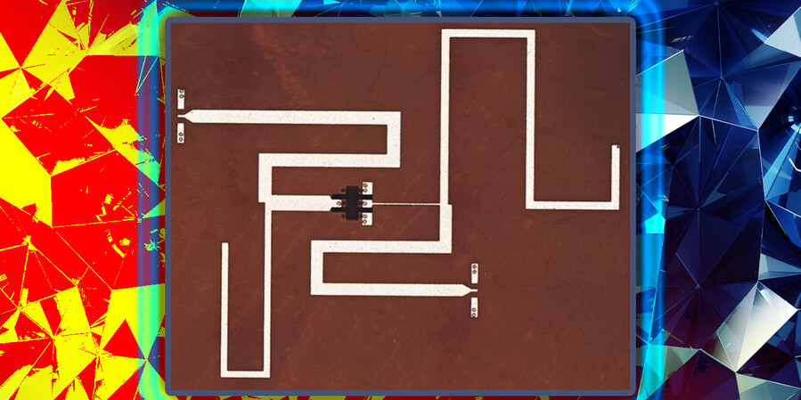
Improving the performance of high-power electronics
Adam Zewe | MIT News
By using a thin layer of diamond to manage excessive heat, researchers can boost the speed and energy-efficiency of next-generation wireless devices.