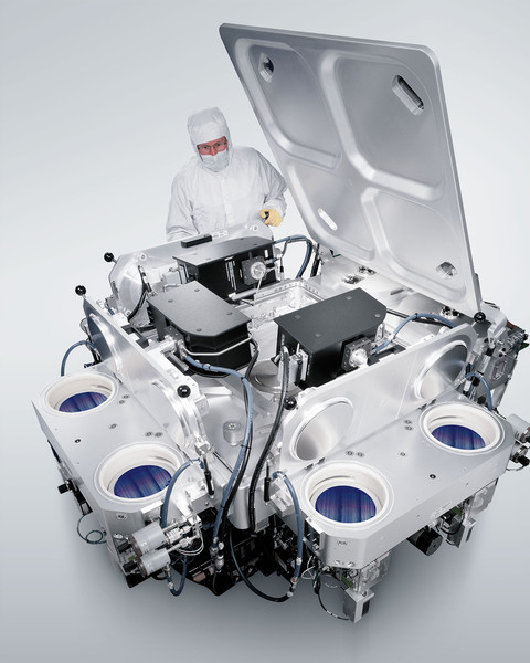
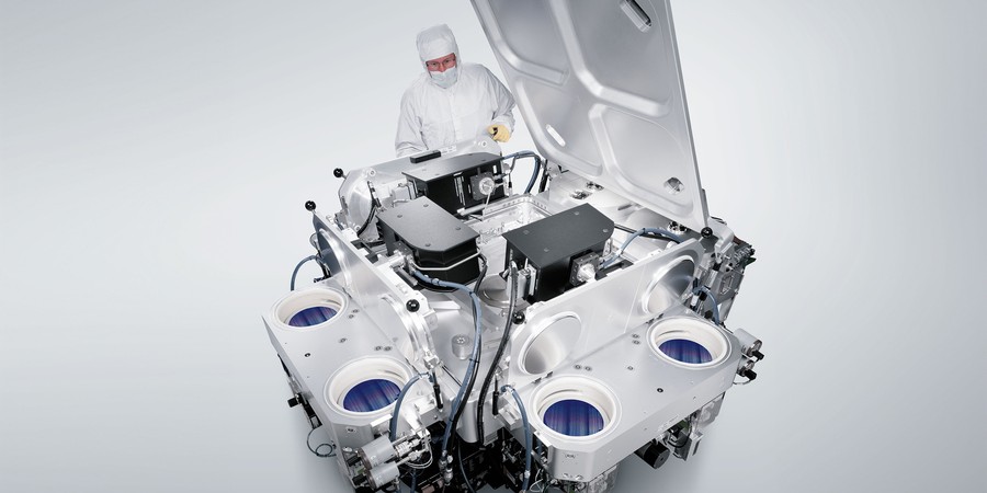
New MIT.nano Equipment to Accelerate Innovation in “Tough Tech” Sectors
Zach Winn | MIT News
The advanced fabrication tools will enable the next generation of microelectronics and microsystems while bridging the gap from the lab to commercialization.
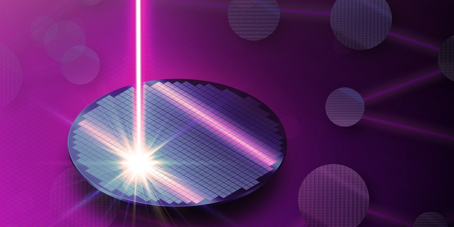
Closing the Design-to-Manufacturing Gap for Optical Devices
Adam Zewe | MIT News
A new method enables optical devices that more closely match their design specifications, boosting accuracy and efficiency.
MIT Group Releases White Papers on Governance of AI
Peter Dizikes | MIT News
MIT has released a new set of policy papers about the governance of artificial intelligence, with aims to help policymakers create better oversight of AI in society.
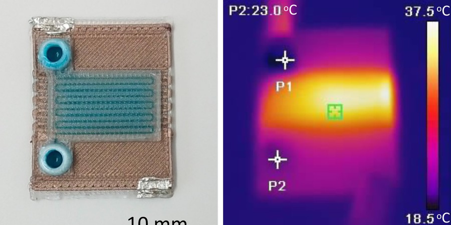
Scientists 3D Print Self-heating Microfluidic Devices
Adam Zewe | MIT News
The one-step fabrication process rapidly produces miniature chemical reactors that could be used to detect diseases or analyze substances.

Researchers Safely Integrate Fragile 2D Materials into Devices
Adam Zewe | MIT News
The advance opens a path to next-generation devices with unique optical and electronic properties.
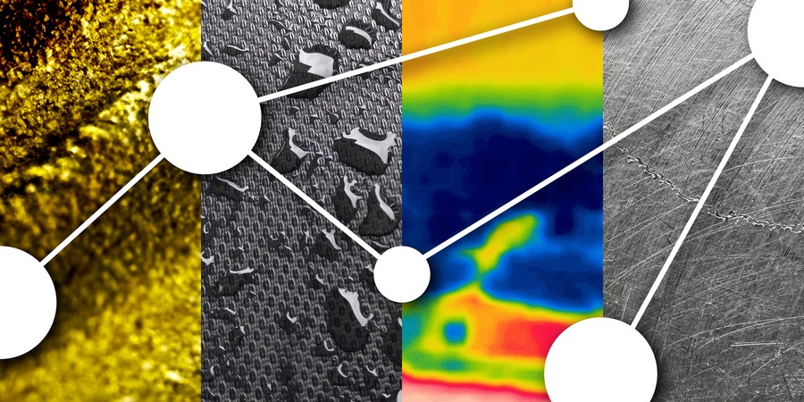
MIT Engineers Develop a Way to Determine how the Surfaces of Materials Behave
David L. Chandler | MIT News
Using machine learning, the computational method can provide details of how materials work as catalysts, semiconductors, or battery components.
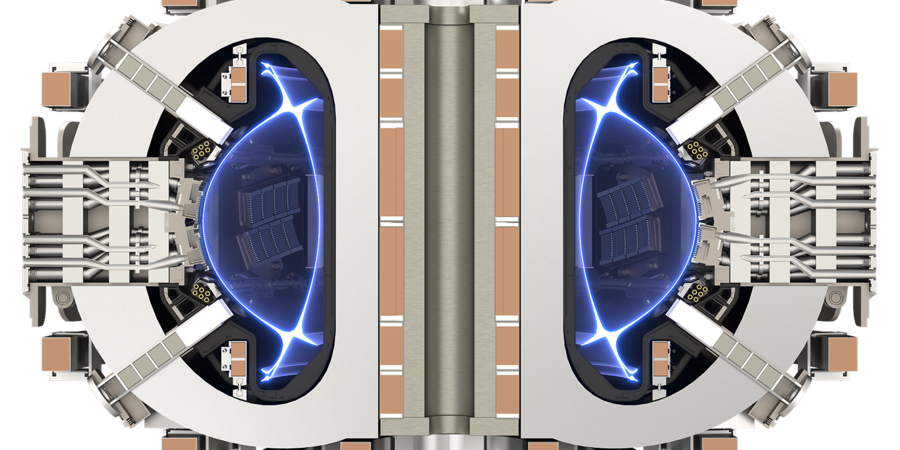
New Study Shows how Universities are Critical to Emerging Fusion Industry
Peter Reuell | Julianna Mullen | Plasma Science and Fusion Center
Fusion’s success as a renewable energy depends on the creation of an industry to support it, and academia is vital to that industry’s development.

With a Quantum “Squeeze,” Clocks Could Keep Even More Precise Time, MIT Researchers Propose
Jennifer Chu | MIT News
Clocks, lasers, and other oscillators could be tuned to super-quantum precision, allowing researchers to track infinitesimally small differences in time, and measure quantum phenomena, including the presence of dark matter.

Celebrating five years of MIT.nano
Amanda Stoll DiCristofaro | MIT.nano
The Nano Summit highlights nanoscale research across multiple disciplines at MIT.
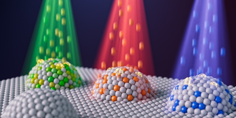
Team Engineers Nanoparticles Using Ion Irradiation to Advance Clean Energy and Fuel Conversion
Elizabeth Thomson | Materials Research Laboratory
Combining the techniques, metal exsolution and ion irradiation, demonstrates control over key nanoparticle properties leading to better performance.